

Understanding The Printed Circuit Board Assembly (PCBA) Process
Regarding modern technology, the world is expanding extremely quickly, and the results are immediately felt in our day-to-day activities. There is now numerous advanced equipment in use that we could not have imagined in past years. However, with the help of these technological innovations, we get to improve our quality of living.
In this article you will learn more about:
Everything from our smartphones and speakers to our automobiles contains electronic components. Every electronic device today includes a printed circuit board (PCB) that allows it to function. Electronics engineering is at the heart of these devices, and the Printed Circuit Boards (PCBs) serve as the core.
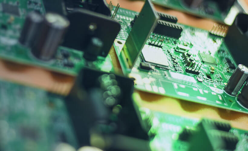
When most people see a printed circuit board (PCB board), they can quickly identify them. These are the green-colored chips with lines and copper bits found at the center of disassembled electronic devices. These boards are made of fiberglass, copper wires, and other metal components. They are epoxy-joined and solder-masked for insulation. This solder mask is the source of its distinctive green color.
An assembled Printed Circuit Board is a PCB with components installed on it, while PCB assembly, or PCBA for short, refers to the manufacturing process. So, how exactly are these electronic devices created? The PCB assembly process is straightforward and includes both automated and manual steps. Below, we've broken down each stage of the PCBA process so you can better comprehend it from beginning to end. Let's get straight into it!
What is PCB assembly?
Different assembly processes are used in manufacturing to create a finished product. The PCB assembly process is one of them. When building an electrical product, manufacturers must consider numerous factors. One of the most crucial factors is how they will integrate components into a working unit that functions as planned. One technology that might be utilized for this procedure is printed circuit board assembly (PCB), which requires meticulous preparation before deployment.
PCB assembly, in a nutshell, is the act of putting everything in one place and constructing something useful from various electronic components. It involves taking a freshly produced board, adding elements and resistors, and then ensuring that it performs as planned. There are several methods for creating PCB assemblies, such as pick-and-place, reflow soldering, wave soldering, etc.
It should be noted that circuit board assembly is distinct from the PCB manufacturing process. PCB prototyping and PCB design are two techniques for making printed circuit boards. Before being used in any electronic device or equipment, a PCB must have Active and Passive Electronic Components soldered onto it. The type of printed circuit board, the kind of electronic components, and the function of the circuit board all affect how these components are assembled.

PCB Assembly and Design Process: An Overview
The base, made up of numerous layers and the most fundamental component of the PCB, is where the PCB assembly process always begins. Each layer is important to the finished PCB's functionality. We will now talk about the many alternating outer layers and their functions.
Substrate
This serves as the PCB's base element -all other components are soldered onto it. It ensures the stiffness and rigidity of the PCB.
Copper layer
A thin layer of conductive copper foil is placed on each functional side of the PCB, either on one side if it is a single-sided PCB or both sides for double-sided PCBs. The copper trace layer is present here.
Solder mask
It refers to the layer applied to the PCB's top and bottom. It provides a distinctive green hue to each PCB. This generates a non-conductive region of PCB, isolating the copper traces from each other to prevent a short circuit. Additionally, it prevents soldering on unnecessary components and ensures that solder only touches pads and holes intended for soldering.
Using a solder mask during printed circuit board assemblies is essential to prevent shorts by preventing soldering to unintended components.
Silkscreen
A PCB board's last layer is a white silkscreen. This layer adds labels to the PCB as characters and symbols. By doing so, the purpose of each board component is more clearly indicated.
On the one hand, according to the substrate material, PCBs can be divided into:
Rigid PCBs
Rigid PCBs are a form of circuit board which are solid and inflexible in their structure. They cannot be bent or flexed, and they are made with a rigid plastic substrate that is usually thicker than standard PCBs. Most PCBs we come across in different types of devices are PCBs. These PCBs come in a range of thicknesses and are robust, rigid, and solid. The main component is fiberglass, often known as "FR4". FR stands for "Fire Retardant - 4." The FR-4 material is advantageous for many hard-core industrial electronic devices because it has self-extinguishing properties. Copper-clad laminates commonly referred to as copper foil laminations, laminate the two sides of FR-4. Epoxies and phenolics, which cost less than FR4, create less durable PCBs.
FR-4 provides:
high dielectric strength electrical insulation
high ratio of strength to weight
Lightweight
relative temperature resistance; therefore, you can anticipate it to function well in most external conditions.
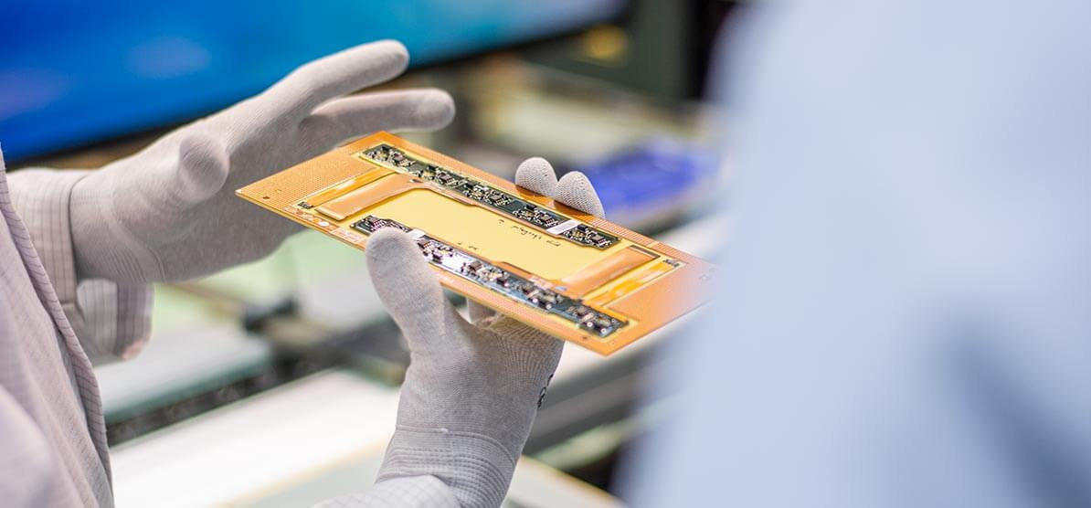
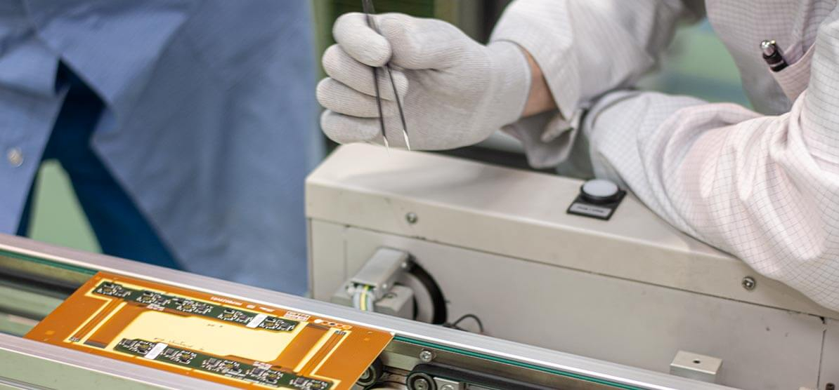
Flexible PCBs
Compared to their more rigid counterparts, flexible printed circuit boards provide more flexibility. A flexible PCB begins by drawing conductive paths onto a dielectric substrate. Each board contains flexible laminates made of special materials to ensure the flexibility of the finished board.
Flexible PCBs offer many advantages over traditional rigid ones: they can be made smaller than rigid boards because they don't need to support their own weight; they can be used in places where traditional boards would not fit; and they can be made out of plastic instead of metal, which makes them cheaper and easier to manufacture.
Types of PCBA Mounting Technologies
The Surface Mount Technology (SMT)
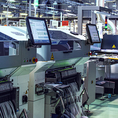
Although it has been around for a while, the Surface Mount Assembly (SMT) market is still flourishing. Surface mount technology involves attaching electronic parts on a PCB board, which can be any size or form depending on your project or product. Pick-and-place machines, ovens, reflow systems, and other PCB surface mount assembly equipment come in varieties. All these components come together to form a circuit board that is wholly functioning and capable of carrying out the specific functions required for your product or gadget.
The surface mount technique is useful for small components and integrated circuits (ICs). Because the surface mount components assembly process is challenging for human hands and can be time-consuming, it is usually performed by automated pick-and-place robots.
The Through-Hole Technology (THT)
THT works effectively on components that require leads or wires to be installed on board by plugging them through holes in the board. The extra lead component must be soldered on the opposite side of the board. This method creates PCB assemblies incorporating big pieces such as capacitors and coils. THT component assembly is typically performed by manual soldering and is reasonably straightforward.
Understanding the PCB assembly (PCBA) Process
Before the actual PCB assembly process can begin, a few preliminary tasks must be completed. This aids PCB manufacturers in determining the functioning of a PCB design and mainly consists of a design for manufacturability (DFM) check. DFM checks can save manufacturing costs and minimize incidental charges by identifying potential problems before they occur.
The actual PCB assembly process involves the following;
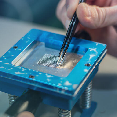
Stenciling With Solder Paste
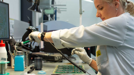
The application of solder paste to the board is the initial stage in PCB assembly. This method is similar to screen-printing a shirt, but a thin stainless-steel stencil is laid over the PCB instead of a mask. The solder paste is a gray substance made up of tiny metal balls, commonly known as solder. These small metal balls comprise 96.5% tin, 3% silver, and 0.5% copper. Assemblers can use this to apply solder paste exclusively to specific areas of the potential PCB. These are the areas on the finished PCB where components will be installed. When heated, this solder paste melts and forms a strong joint.
Pick and Place
Following solder paste application to the PCB board, the PCB assembly process proceeds to the pick and place machine, a robotic device that sets surface mount devices, or SMDs, on a prepared PCB. SMDs now account for the majority of non-connector components on PCBs.
Traditionally, this was a manual operation that required assemblers to pick and place components by hand using a pair of tweezers. This procedure is now, thankfully, an automated process among PCB assemblers. This transition mainly occurred because machines are more accurate and consistent than humans.
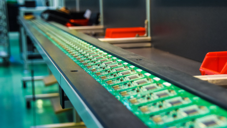
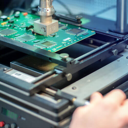
Reflow soldering
Once the solder paste and surface mount components are in place, they must remain put. This means that the solder paste must solidify before components may be attached to the board. This is accomplished by a process known as "reflow."
The reflow soldering process involves placing the PCBs and components on a conveyer belt. This conveyer belt transports the PCBs and components into a large oven heated to 250 degrees. This temperature causes the solder to melt. Melted solder will then adhere the components to the PCB and form joints. After being subjected to high temperatures, the PCB is placed in cooling. The solder junctions are subsequently solidified in a regulated manner by these coolers. This will form a permanent connection between the SMT component and the PCB.
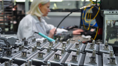
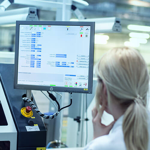
Quality Control and Inspection
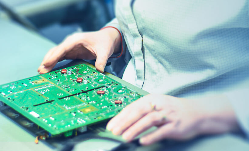
After the components are soldered in place during the reflow process, the PCBA is not complete, and the finished board must be checked for functionality. After reflow soldering, there is a potential that the components become misaligned as a result of erroneous movement in the PCB holding tray, resulting in a short circuit or open connection.
The three examination methods used are manual inspection (this technique is practical for boards with THT components and a lower component density), optical inspection (which uses an automated machine outfitted with high-powered, high-resolution cameras positioned at various angles to view solder connections from multiple angles), and X-ray inspection (which allows the observer to see through layers and visualize lower layers to identify any potentially concealed issues and commonly used for more complex or stacked PCBs).
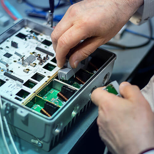
Fixation and Soldering of THT Components
Through-hole components can be found on many PCB boards. These parts are also known as Plated through Hole components (PTH). The leads of these components will travel through the hole in the PCB.
PCB components use these holes to transmit signals from one side of the board to the other. Soldering paste will not work in this situation since it will run right through the hole with no possibility of adhering.
In the subsequent PCB assembly process, PTH components need a more sophisticated type of soldering technique in place of soldering paste:
Manual through-hole insertion is a simple procedure that requires manual soldering. Typically, one person will insert one component into a specific PTH at a station. When they're done, the board is moved to the station below, where a different individual attempts to attach another component. For every PTH that needs to be equipped, the procedure is repeated.
Wave soldering is the automated equivalent of the manual soldering method but uses an entirely different procedure. This time, a wave of molten solder is applied to the bottom of the board when the conveyor belt passes through a specialized oven. Because wave soldering the entire PCB side would render any fragile electronic components worthless, it is practically impossible to use it for double-sided circuit boards.
Final Inspection and Functional test
The PCB is now prepared for inspection and testing. This is the functionality test, in which the PCB is supplied with electrical signals and power at the designated pins, and the output is examined at the designated test points or output connectors. Standard laboratory tools, including an oscilloscope, a DMM, and a function generator, are needed for this test.
Final cleaning, finishing, and shipping
This is the last step in the PCB assembly process. With the PCB examined and deemed to be in good condition overall, it is time to remove any remaining flux that isn't wanted as well as finger dirt and oil stains. All forms of dirt can be removed with a high-pressure washer made of stainless steel and deionized water. After washing, compressed air is used to dry the PCB. The finished PCB is now prepared for packaging and shipping.
A partner you can trust!
By choosing VECTOR BLUE HUB as your cooperative PCBA provider, you're deciding to work with a company that offers the best results. Our PCB assembly services adhere to the strictest standards of quality. Whether it's a double-sided or single-sided PCB, an SMT, through-hole, or a mixed-assembly project, we can handle it.
VECTOR BLUE HUB has been offering its clients high-quality printed circuit board assemblies by continuously evaluating their wants and needs. Contact us today, and let's get you through a smooth-sailing PCB assembly process while you save time and money!