

BGA Chips - Technology and Applications
Modern electronics, where smaller sizes and increased capabilities are in demand, stimulated the development of Surface-Mount Technology (SMT). However, as demand grew, there was a requirement for faster assembly and higher-density technologies to accommodate these items.
Ball Grid Array chips play a crucial role in this. These small wonders are the heroes that enable devices we rely on daily such as smartphones, laptops, gaming consoles and automotive systems.
This article discusses all you need to know about a BGA package They are frequently seen in the most recent CPU microprocessor packages.
BGA chips are often built from a multilayer printed circuit board (PCB) with solder balls affixed to the board to represent each integrated circuit link., extending to their structure, advantages, applications, challenges and role in technological advancements.
What is BGA Chip?
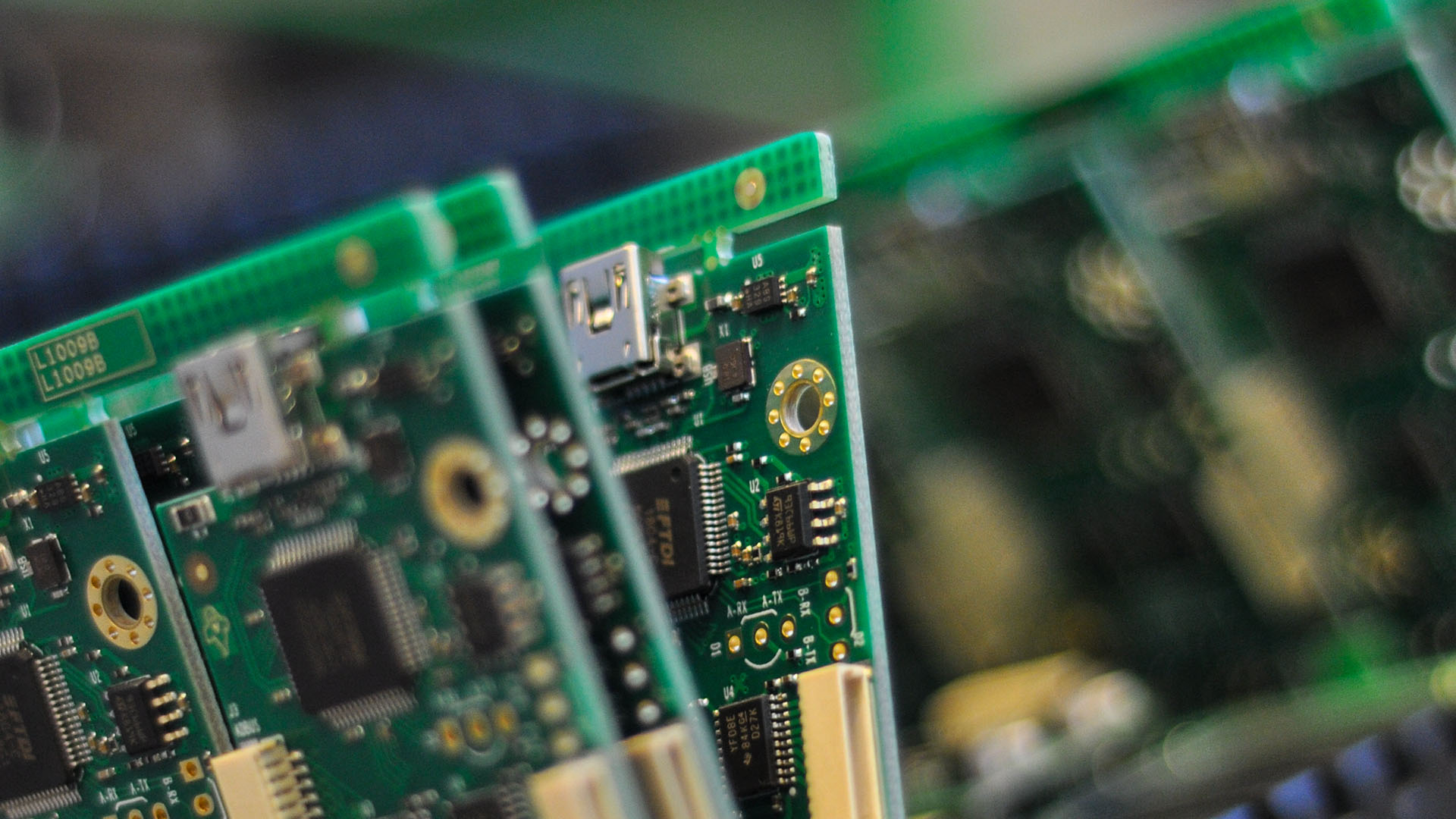
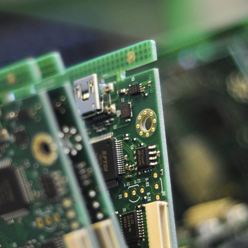
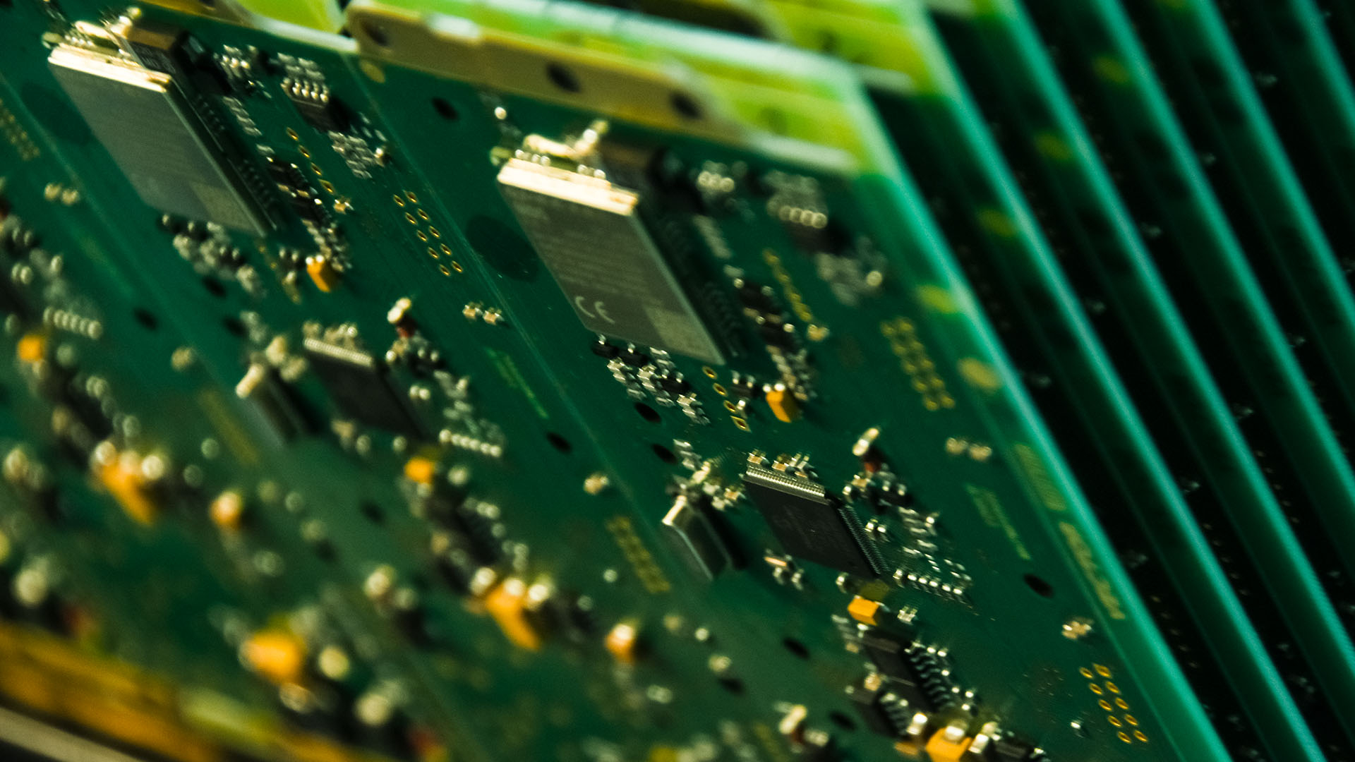
A Ball Grid Array (BGA) chip is an invaluable surface-mount packaging technology that is crucial to integrated circuits (ICs) in electronic devices. BGA chips have revolutionized the way electronic components interact and perform. A BGA chip is a circuit packaging type that is used to mount and connect microchips to printed circuit boards (PCBs).
BGA chips are made up of an integrated circuit put on a substrate with an array of solder balls on the bottom that connects to a PCB. The grid arrangement of the solder balls gives the package its name. Unlike Surface Mount Technology (SMT), which solders the chip legs to the PCB, BGA chips contain a grid of solder balls attached to the backside. The legs are replaced with these solder balls, which are constructed of either lead-based or lead-free materials.
BGA is the most common type of IC packaging and can be found in a variety of electrical applications. BGA packages are the smallest packages available and may fit a significant number of pins on the chip. They are frequently seen in the most recent CPU microprocessor packages.
A BGA socket has a rectangular plastic shape and has specific slots on its undersides that fit each solder ball of the BGA chip appropriately. The importance of BGA sockets regarding BGA chips is seen in their ease of PCB surface installation. By eliminating the difficulties involved in individually finding and soldering IC pins onto the board, these sockets simplify the mounting of BGA chips onto PCBs. The use of BGA sockets offers a solution that eliminates the mounting process's potential for annoyance and time-consuming nature.
These sockets come in two different types: passive and active. Active BGA sockets include electrical contacts that serve as the solder balls' connecting points to the BGA chip. These connections create the crucial relationship that ensures efficient operations and operational integrity. A passive BGA socket does not have any contact pads on its underside.
What are BGA chips made of?
The BGA chip package is rectangular and typically houses a single die positioned at its centre. This configuration comprises two interconnected bga components: the core and substrate.
The core serves as a foundation, crafted from either metal or ceramic, providing sturdy support for the active device(s). As for the substrate, it's typically fashioned from glass or plastic and is adorned with preformed solder balls.
It is available in two varieties: unidirectional and bidirectional. There are no solder balls in all directions of the PCB tracks in a unidirectional BGA, but only one direction contains solder balls. There are solder balls in both directions of the PCB rails in a bidirectional BGA.
BGA chip features several connectors on the chip's backside, and these are soldered to the device's PCB. BGA chips include both male and female connectors. The male BGA connection is carefully constructed to interact flawlessly with its female counterpart. It is important to remember that using a female BGA connection to connect a male BGA component to a PCB may cause poor performance or even circuit damage owing to probable short circuits.
Putting both connections on top of the PCB before starting the process ensures that the male and female connectors are perfectly aligned. This proactive step improves accuracy and guarantees a secure connection.
What does a typical BGA chip look like?
The components of Ball Grid Array chips include the following:
Die
The die is the basic semiconductor bga component that is in charge of carrying out its assigned function. It includes a variety of electronic components such as transistors, resistors, diodes, capacitors, and others. The die is often made of silicon and is protected by a layer of silicon dioxide or 'oxide,' which acts as a barrier against external impurities. Wire bonding, a process that assures secure connection, is used to link the die to the BGA package substrate.
BGA Package
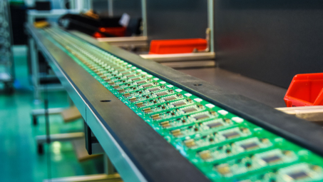
BGA packages serve as the container for all of the BGA chip's constituents, with a solder ball-adorned substrate. These solder balls operate as the BGA package's electric connections, producing a complex grid on the PCB's surface.
The number and density of solder balls depend on the size of the BGA package. A 0.5 mm pitch BGA, for example, holds around 15,000 solder balls, as opposed to a 1 mm pitch variation that retains 3,000 solder balls. The potential of BGA packages to improve performance while saving space is the key reason for using them. As a result, they are well suited to high-density interconnect applications such as CPU microprocessors and memory chips.
BGA packages have excellent mechanical durability. Instead of solder, the balls are often attached to the chip using a little amount of adhesive. This function prevents any damage to the mechanical structure by accommodating minor discrepancies between the balls and the chip's contact pad. Subpar electrical connections may occur in situations of significant misalignment, perhaps resulting in solder fatigue.
Substrate
The BGA package is connected to the substrate using it as a support. It consists of a thin glass or plastic layer with a top layer that holds the substrate in place and a base layer that covers the solder balls. Depending on the requirements, this top layer may be made of different materials including copper, aluminium, nickel, or titanium.
Pitch
The number of solder balls in a particular square inch is known as the pitch. Essentially, it is the number of solder balls that are attached inside a one-square-inch region of the PCB. Pitch values vary across various BGA packages, depending on the manufacturer's particular requirements.
Solder Ball
They are tiny, spherical balls of solder that surround the surface of the substrate in a grid pattern. They serve as the electrical contacts of a BGA package.
Each ball in a BGA package is attached to the core substrate using a liquid epoxy-type of adhesive. The liquid epoxy adhesive must be heated to a specified melting temperature depending on its composition to cure. But the BGA package cannot be used during the downtime that this curing procedure causes. The pitch and ball size of the BGA package are closely correlated to the quantity and solder balls.
Trace
The trace is what connects the component to the motherboard within the BGA chip pack. It serves to transport signals from one component to another on the PCB using copper wires.
Another set made by manufacturers is trace width, which varies amongst BGA packages to satisfy different purposes.
Advantages of the BGA Chips
Small in Size
A BGA chip is specially designed to take up the least amount of room on the circuit board, making them a standout option for small devices. This clever layout not only saves space but also makes allow for denser and more complex circuit combinations.
There are no protruding leads that take up extra room since the electrical connections are made by solder balls on the package's base. This compact size makes it possible to utilize the board space more effectively and makes it easier to create electrical bga devices that are both thinner and smaller.
Self Alignment
The BGA chip's solder joints are designed to be spherical, which naturally aligns with the packaging and ensures exact alignment when the chip is mounted on the circuit board. The BGA chip's dependability is increased by this built-in alignment mechanism, which reduces the possibility of mistakes and inconsistencies during manufacture.
Cost Effective
Higher manufacturing yields are made possible by the BGA chip's architecture, which lowers production costs. The BGA chip is a cheaper alternative to other chip types because of this, as well as the simplicity and cost of the rework and desoldering process.
Easy to Desolder
The reworking and desoldering process is made easier by the larger solder pads that come with them (using a solder bath or hot air). This quality speeds up repairs and replacements, which ultimately cuts downtime and related repair costs.
Better Conductivity
A BGA chip has more conductivity than other chip varieties because of its small size and multiple joints. The reduced likelihood of signal interference caused by this increased conductivity makes BGA chips the best option for high-speed and high-frequency circuits.
Powerful Thermal Dispersion
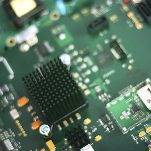
BGA chips are better in terms of heat control. The chip stays cool and performs at its best because of its design, which enhances heat transmission efficiency. BGA chips can also be used in conjunction with extra heat-dissipation components like heat sinks or thermal vias to improve their capacity for thermal management.
Disadvantages of BGA Chips
While BGA packages offer numerous advantages, it's important to acknowledge their drawbacks in comparison to pin-based packages:
The method of soldering each contact point, or ball, to the PCB is a crucial component of BGA packages. The solder balls are melted at temperatures over 400° C (750° F). Sadly, the substrate material may suffer damage at these high temperatures. Because bigger packages can be used in situations when a small package size is not necessary, BGA packages are rarely used in those situations. BGA packages might not be the best option for situations where dependability takes precedence over size considerations.
Large temperature differences across the ball as a result of poor thermal contact between the ball and substrate may lead to solder fatigue and unreliable operation or even damage to the IC. The BGA must be connected to a heat sink or a PCB flat on its side. The temperature produced by the soldering operation may be too high for the substrate to handle. To disperse the heat in this situation, the chip must be fastened to a heat sink made of a material with strong thermal conductivity.
Extra power used when handling the balls may cause them to separate. Even though the adhesive securely fastens the balls to the substrate, any separation might cause issues. A detached ball is difficult to find and recover, which compromises dependability in addition to being risky. Visual examination alone could be insufficient when dealing with the complex grid of solder balls and connections in a BGA package. X-ray inspection of the BGA offers a non-destructive method to see within the internal structure in situations like these.
Does the BGA chip need solder paste?
Yes, before going through the assembly process, the BGA chip needs solder paste applied to the PCB pads. A key component is solder paste, which is made up of a mixture of solder balls and flux. Notably, BGA paste has a range of melting temperatures and a smaller diameter. With the use of a stencil, this solder paste is carefully placed on the PCB's pads. There are pads on the BGA chip that are either connected or soldered to other pads on the board.
The BGA chip is carefully positioned on a bed of solder ball paste during assembly, then it goes through a controlled heating procedure to start melting. A solid and reliable connection forms between the BGA chip and the appropriate PCB pads when the solder balls melt.
Conclusion
VECTOR BLUE HUB is one of the leading partners in electronic design and manufacturing. Our primary goal is to help our esteemed customers obtain great products while maintaining cost-effectiveness. Any questions you may have about BGA chips and their unique features are warmly welcomed. Feel free to contact us today!