

Precision and Perfection: Exploring the Intricacies of PCB Prototype and Assembly
Every functioning electronic device is powered by a core—the printed circuit board (PCB). Printed Circuit Boards (PCBs) are the framework of the electronic components, and they make it possible to connect the internal components.
A printed circuit board (PCB) prototype is a preliminary form of a printed circuit board (PCB) used for testing and assessing designs prior to manufacturing. Before beginning a major electronics project, PCB prototypes can be manufactured in small quantities or as single boards to check that the design fulfils the required standards and performs properly.
The importance of prototyping in PCB design cannot be overexaggerated. The PCB prototyping process is essential for producing electronics, allowing manufacturers to test their concepts and designs before mass production. Simply put, it serves as a sturdy preliminary Proof of Concept (POF) before the final manufacturing process.
So, what does the PCB prototype and assembly process entail? Continue reading to figure it out!
- What Is Prototype PCB Assembly?
- Benefits of PCB prototype assembly
- 1. Design validation
- 2. Quality assurance
- 3. Component compatibility
- 4. Cost-effectiveness
- 5. Time savings
- Process of PCB Prototyping and Assembly
- Step 1: Designing the PCB
- Step 2: Design Preparation
- Step 3: PCB Prototyping
- Step 4: Testing and Debugging
What Is Prototype PCB Assembly?
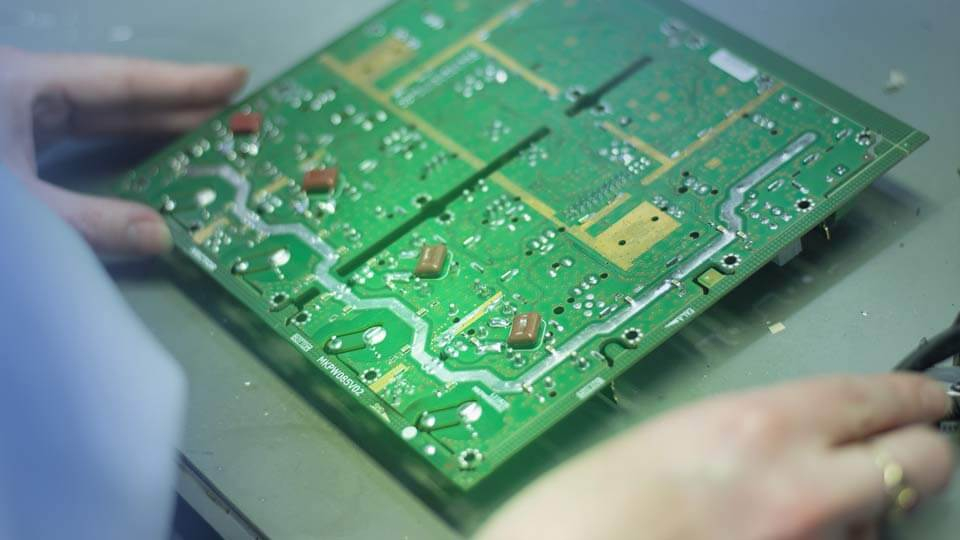
Prototype PCB assembly is a critical phase following the PCB design process, validating the design’s feasibility and identifying potential issues. During this phase, the manufacturer performs a comprehensive analysis of the board’s strengths and weaknesses, which serves as a reference for future versions. Prototype PCB assembly is a crucial step in the overall PCB manufacturing process, enabling manufacturers to gain a comprehensive overview of the entire process and eliminate any errors before commencing full-scale production. Manufacturers can ensure that the final product functions optimally during mass production by conducting rigorous testing during the prototype phase.
A prototype PCB is generally a simplified, elementary iteration of a final production board, often lacking advanced features and design embellishments. Despite this, it must be a precise, top-quality, fully operational test version of the completed PCB. During prototype PCB assembly, it is critical to replicate the fundamental design, functionality, and component load-out of the final production run as closely as possible to minimise discrepancies.
Errors or omissions during this phase can result in significant expenses if not addressed before proceeding to full-scale PCB manufacturing. Hence, executing a PCB prototype with precision and accuracy is imperative.

Benefits of PCB prototype assembly
There are several benefits of PCB prototype and assembly compared to delving right into mass production, including:
1. Design validation
PCB prototype and assembly make it possible to verify and validate the design before proceeding to full-scale manufacturing. This process identifies any errors or issues and offers an opportunity to refine the design for optimal performance. A well-crafted PCBA prototype serves as an excellent indicator of what to expect from the final product during mass production. This is because the prototype’s performance reliably reflects the final product’s functionality. Moreover, by scrutinising the PCBA prototype for faults, manufacturers can refine the PCB and its components, thereby enhancing the final product’s overall quality. In essence, a meticulously assembled PCBA prototype provides valuable insight into the final product’s performance and an excellent opportunity to iron out any issues before going into full-scale production.
2. Quality assurance
It provides an opportunity to test the quality and reliability of the board. This testing ensures that the board meets the required specifications and standards and performs reliably under different conditions, allowing for a more smooth-sailing PCB manufacture and assembly process.
3. Component compatibility
With PCB prototyping, developers can test the compatibility of the electronic components to be used on the board. This testing ensures all components work together efficiently and effectively, minimising the risk of failure during operation.
4. Cost-effectiveness
Manufacturers can save significant costs by identifying design errors and issues early in the process. This early identification allows manufacturers to make the necessary corrections before proceeding to full-scale manufacturing, minimising the risk of costly mistakes.
5. Time savings
This stage reduces the time required for testing, validation, and the overall production process. This reduction in lead time results in faster time-to-market for the final product.
Process of PCB Prototyping and Assembly
Step 1: Designing the PCB
The first step is to create the PCB. A schematic, or graphical circuit representation, is created throughout the design process. The schematic depicts all the circuit’s components and their connections. The layout, which is a physical representation of the PCB, is the following phase. Layout entails arranging the components on the PCB and routing the traces that connect them.
Step 2: Design Preparation
After the PCB design is finished, the design is ready for prototyping. This stage entails creating Gerber files, the industry-standard file format for PCB manufacture. The Gerber files include all the information needed to construct the PCB, such as the trace width, spacing, and drill holes. The Gerber files are subsequently forwarded to the PCB manufacturer.
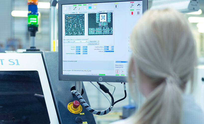
Step 3: PCB Prototyping
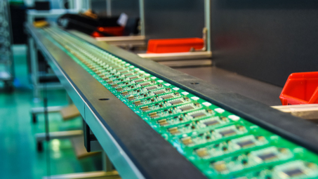
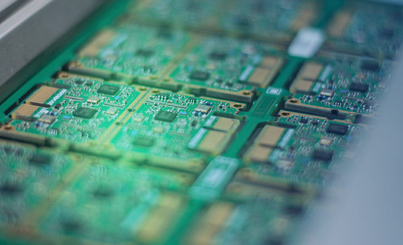
This involves manufacturing a small batch of PCBs to test the design’s feasibility and identify any issues. The prototype should accurately represent the final product with the same components and design features. It involves several stages, including:
a) PCB Manufacturing and Copper Plating: This stage involves applying a layer of copper to the PCB substrate and etching away the unwanted copper using a chemical process. The remaining copper forms the traces that connect the components.
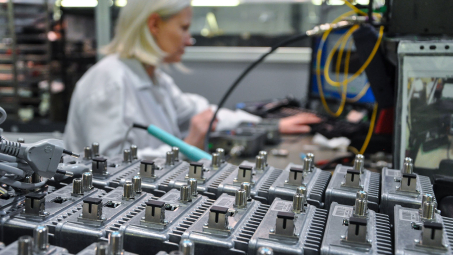
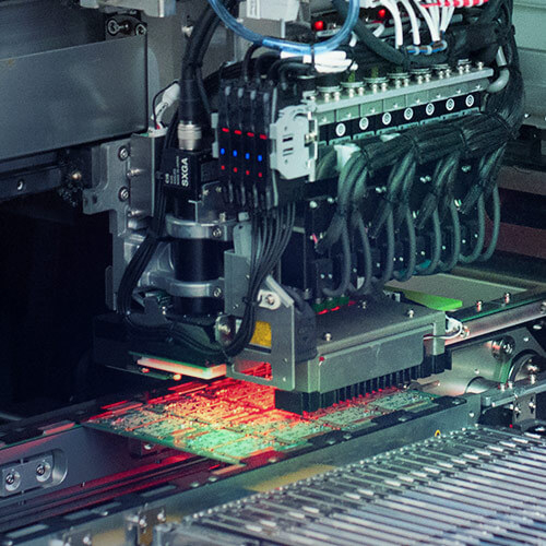
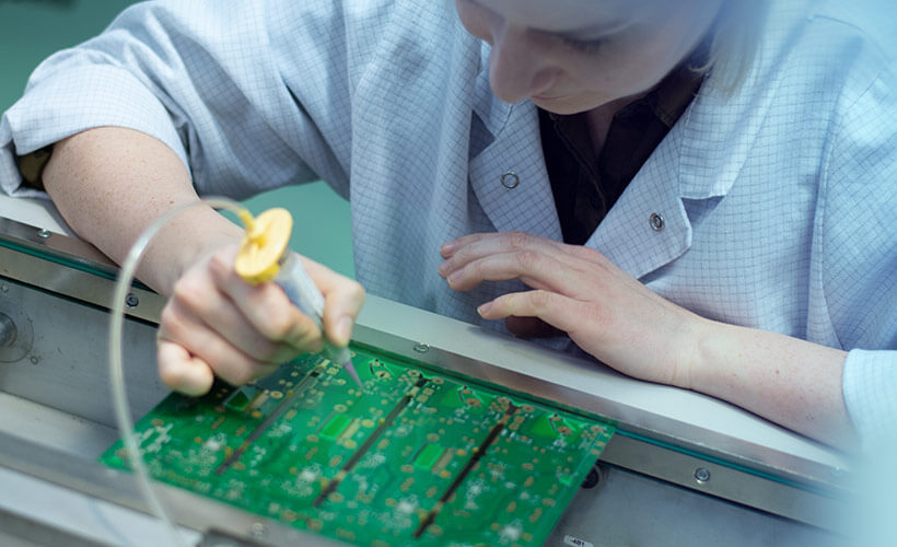
b) Component Placement: This stage involves placing the components on the PCB using a pick-and-place machine. The pick-and-place machine picks up the components from the feeder and places them on the PCB according to the design.
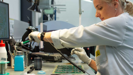
c) Soldering: This stage involves attaching the components to the PCB using solder. In this stage, the printed circuit board is positioned on a moving belt which carries it through a reflow oven. There are two types of soldering techniques: through-hole and surface mount. Through-hole involves inserting the components through holes in the PCB and soldering them on the other side. Surface mount involves attaching the components directly to the surface of the PCB.

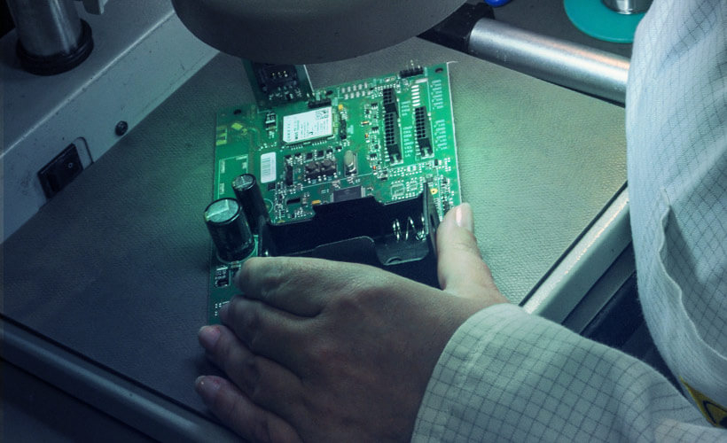
Step 4: Testing and Debugging
You have a finished prototype once it has been conceptualised, built, and assembled. Before going on to a full production run of your PCB, it is now time to test it.
Test the prototype in line with your intended use. Look for design errors and potential areas for improvement. Do identical tests on the boards if you have many prototypes of various designs, then compare the findings. Tests may show issues with your design, which means you will need to fix them and maybe make a new prototype. If no errors are found, you can go ahead with mass production of the PCBs.
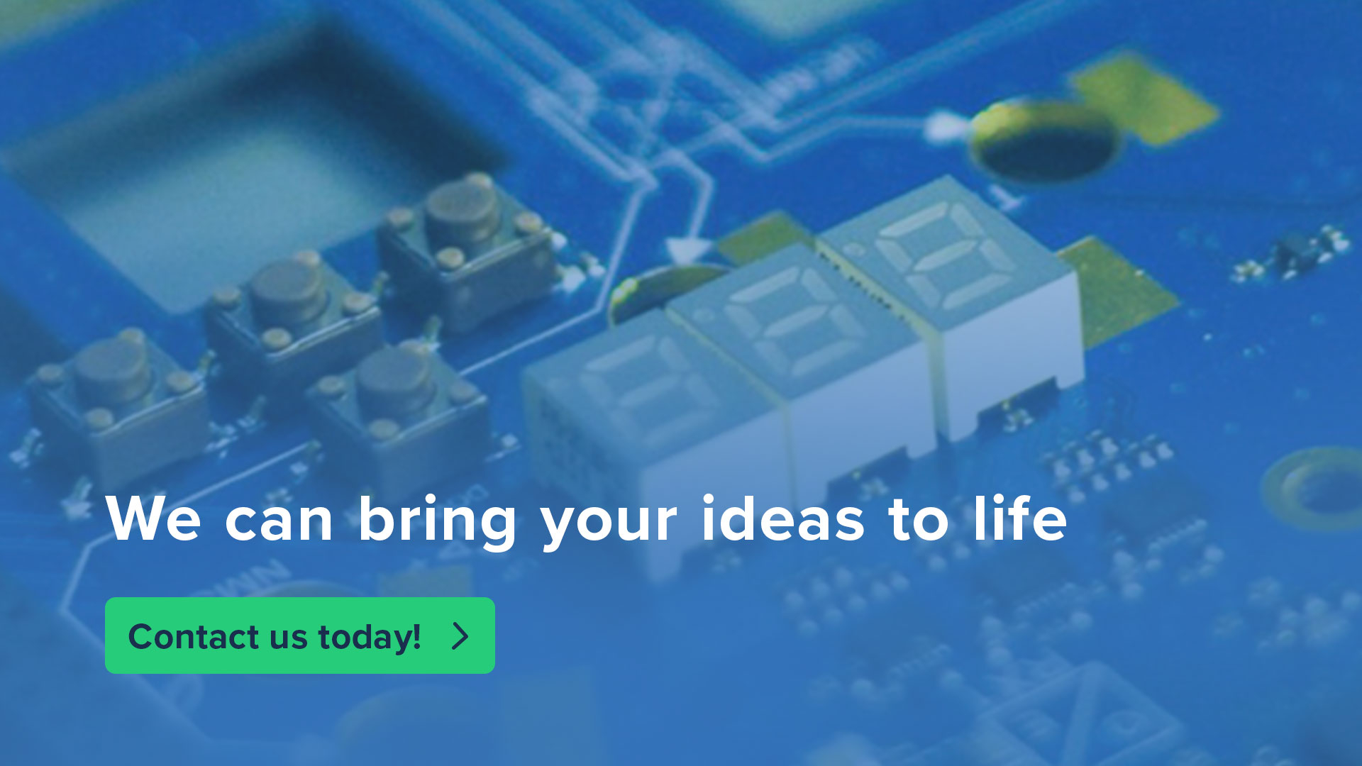
Work with VECTOR BLUE HUB today!
Creating high-quality PCB prototypes is a daunting task that demands technical expertise. Hence, it would be best to collaborate with a trusted expert like VECTOR BLUE HUB.
With years of hands-on experience in the EMS industry, we are a leading partner for all your electronic prototyping needs, and everything in between. Whether you have a small or large project, we have the expertise to handle everything.
Our team of qualified and experienced electronic manufacturers is equipped to bring your ideas to life. We pride ourselves on our commitment to providing top-notch services and ensuring that each project meets the highest standards of quality.
Trust us to deliver excellence in electronic prototyping.