


How are PCBs made? A Beginner's Guide to the PCB Manufacturing Process

Manufacturing electronic components and devices is a very intricate process. Take phones, for example: From the screen to the frame and communication devices, each component is extremely intricate and has seen decades of research go into it. One component, however, stands above the rest and acts as the heart of most electronic devices, and that's the printed circuit board (PCB). From smartphones and laptops to household appliances, without the PCB, none of these devices function at all.
Whether you're a tech enthusiast, an aspiring engineer, or simply interested in the inner workings of your favourite electronics, understanding how PCBs are manufactured is an essential tour into the very essence of modern electronics production. But it doesn't end there: even though the first PCB was invented a century ago, the technology behind them keeps advancing. The wires on PCBs are getting thinner, boards are getting more complex to handle all the electrical connections modern devices need, and design best practices keep changing to better accommodate newer, tinier electronic parts. Even the way they're put together is changing.
Despite all these changes and despite all of the different ways circuit boards are manufactured, they all follow similar, if not identical, steps. In this guide, we'll take you through the printed circuit board manufacturing process from A to Z. How PCB is made, the out layers, the copper layer, and the electronic components: You'll learn about these and more once you finish reading this article!
Background: The Basics of How Circuit Boards Are Made
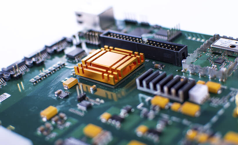
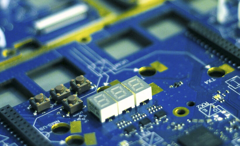
Printed circuit boards, often known as PCBs, are found within various devices, from simple beepers and radios to powerful radar systems and computers. These circuits are created by placing a thin layer of conductive material onto an insulating board, called the substrate material. Tiny electronic components are then put onto the substrate and connected to these circuits through soldering.
Printed circuit boards, or PCBs, come in various forms. There are three main types:
- single-sided circuit board,
- double-sided circuit board,
- multilayer circuit board.
A single-sided board has components on just one side of the substrate. When there isn't enough space to fit all the components on a single-sided PCB, a double-sided circuit board is used. Holes drilled into the substrate connect the circuits on both sides of the board, which are coated with conductive material.
The third type, a multi-layered board, is like a sandwich with layers of printed circuits separated by insulating layers. The components on the outer layers of the circuit board connect through holes that are drilled down to the right inner layer. Though the circuit pattern is more straightforward in single and double-sided boards, the clever use of multilayered circuit boards makes many modern devices possible.
Although all three types are quite different, the manufacturing process diverges only after the initial layer is created, and it is then that the level of complexity truly shows. Depending on the form, size, and number of layers of the PCB, the circuit board manufacturing process might comprise 20 or more separate phases.
Naturally, the more complex is a printed circuit board, the more steps are needed to make it. Think of it like building a puzzle – every piece has to fit in just right. In the case of PCB manufacturing, if you skip or simplify any of the steps, it can cause big problems in the finished PCB, sometimes resulting in total malfunction. On the other hand, when each step is done carefully and precisely, the resulting PCBs are reliable and durable, becoming the backbone of many electronics we know and love!
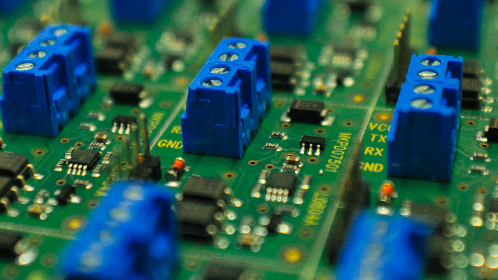
Key Parts of a Printed Circuit Board
When "how are printed circuit boards made" is asked, the first topic we need to explore is the basic building blocks of the PCB. Whether it is for housing, communication, or insulation, these building blocks are key to how the PCB and its many components function. Just like a house, if you don't get the basic building blocks right, the whole thing will come crashing down.
A standard PCB is made up of the following key parts:
- Substrate
This is the backbone of the PCB, the core base of its primary layers. The most common material used to make PCB substrates is fibreglass-reinforced epoxy resin (FR-4) copper foil because of its strength and durability. Ceramic-filled PTFE composites (e.g., Rogers RO3003) are used for PCBs that are used in devices with high-frequency applications. Meanwhile, cyanate ester or polyimide (e.g., Panasonic TR-77) are employed in high-temperature situations. Less costly alternatives, such as paper-reinforced phenolic resin with bonded copper foil, are also utilized in certain circumstances, particularly in domestic electrical pieces of equipment where affordability is key!
- Prepreg
The prepreg is like the glue that holds everything together. It is made of glass fibre cloth that has been soaked in partially cured epoxy and is used to glue the PCB layers together under heat and pressure. The prepreg is positioned beneath the substrate layer, and beneath it, a copper sheet is added.
- Metal Foil
It's a thin copper foil that's shaped into conductive traces and pads. The thickness can vary. The copper foil is necessary for its electromagnetic shielding and antistatic properties. Not only does its thickness vary, usually ranging from 0.5 oz (17 μm) to 3 oz (105 μm), but it can come in single-side, double-side, and self-adhesive varieties depending on the type of the printed circuit board.
- Coatings
The coatings act as the PCB's protective coating - its skin, to make an analogy. There are many types of coatings, and they are chosen depending on the type of environment the printed circuit board operates. The most common are solder masks, which protect the copper from contact with the environment, and silkscreens, which display data like as component numbers, logos, symbols, switch settings, and test points.
- Bonding Film
Bonding films, or bonding sheets, are commonly used in multi-layer PCBs and perform several functions, including protecting wiring and other fragile elements, thermal insulation, and static protection. In many ways, they are similar to the glue used in the lamination of multi-layer PCBs.
- Vias and Via Fills
Vias are tiny holes that allow multiple layers of a printed circuit board to communicate. In high-density interconnect boards, vias are frequently filled with plating resins or conductive pastes to provide additional protection and insulation. The contents of the resin, the aspect ratio of the hole, and the thickness of the core are all important considerations when vias are designed on a PCB.
These are just the building blocks of PCBs, you have to remember! A complete PCB also includes many other components like resistors, capacitors, transistors, diodes, and integrated circuit chips, which provide functionality and enhance the reliability of the PCB.
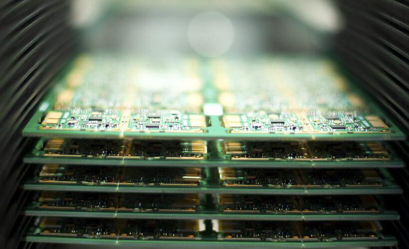
Steps in the Manufacturing Process of Printed Circuit Boards
The PCB manufacturing process begins with blueprints, goes through a complex multi-stage manufacturing stage, and ends on a functional PCB. Each step is vital and builds on earlier steps of the process, and this is why when discussing how are PCBs manufactured, we need to have a holistic picture of the process as a whole. In this section, we'll go through every step in detail:
Step One: Designing the PCB
The printed circuit board manufacturing process begins with a design phase where engineers and designers use specialized software, such as Extended Gerber (IX274X), to create a blueprint that outlines the PCB's layout and requirements. PCBs come in many forms, shapes, and variants, and the PCB design, layout, component, and properties all need to perfectly match the needs of the device the PCBs are intended for. This is why a thorough research and designing phase is how the process begins.
The software used during this phase is also vital. Not only do they aid in designing, but they also encode essential information like the number of copper layers, solder masks, and component notations, which are needed before the product enters mass production.
Step two: Design Review and Engineering Considerations
After the initial design, the PCB undergoes a thorough examination to ensure error-free specifications. In this stage, engineers rigorously assess the PCB design to look for any potential defects, missing components, or structural difficulties.
Any uncaught mistakes during this stage will prove quite costly at later stages. At a minimum, new circuit board designs need to be created, prototyped, and tested, and in some unfortunate circumstances where mistakes persist into the mass manufacturing phase, the entire product launch could end in failure.
After engineers review the PCB design meticulously to check for any potential errors, missing components, or structural issues, the design is approved by the engineering team, and we proceed to the printing phase.
Step Three: Printing the PCB Design
The PCB design is printed using a special type of printer known as a plotter printer. This printer creates a "film" of the PCB design, somewhat resembling transparencies. The inner layers of the PCB are represented using two ink colours: black ink for copper traces and clear ink for non-conductive areas. Clear ink denotes copper pathways on the outer layers, while black ink represents areas where copper will be removed. Registration holes are punched through the printed films to aid alignment in subsequent steps.
While computer software and simulation have come a long way and are a key part of the circuit board design process, due to how costly mistakes can be, they alone aren't enough to ensure no mistakes have been made. The printed PCB design gives further opportunity to ensure proportions, wiring, and components are correctly placed.
Step Four: Creating the Printed Circuit Pattern
The next phase is to create the printed circuit pattern, which is done by copper plating the conductive pattern and a layer of positive photoresist material is vacuumed onto the foil surface. The printed circuit pattern mask is placed on top and exposed to ultraviolet light causing the photoresist material within the circuit design to become soluble. The circuit pattern mask is removed, and the board is treated with an alkaline developer, revealing the exposed copper foil circuit design.
Step five: Chemical Etching Process of the internal layers
Before proceeding, extra and unwanted copper on the PCB's inner layers must be removed. The board is etched by exposing it to a chemical solution that eliminates the exposed copper while keeping just the needed copper traces intact. Depending on the design, the time and intensity of the treatment may vary. The process of removing unwanted copper needs to be done in a tightly controlled environment to ensure other parts of the PCB aren't damaged.
The purpose of this step is to ensure the width of the conductor matches the blueprints exactly.
Step Six (For Multilayer PCBs only): Inner Layer Processing
In this step, the inner layers of multilayer PCBs undergo a series of processes. This includes imaging, etching, resist stripping, post-etch punching, automated optical inspection, oxide application, layup, and lamination. These procedures ensure proper layer alignment, etching, and insulation for a functional multilayer PCB.
Step Seven: Align the Layers
Next, we need to make sure the layers of the PCB are perfectly aligned using registration holes. An optical punch machine aids in performing this take.
There is a very intricate interplay between the outer layers and the inner layers of the PCB, and slight misalignments will not only hurt the performance and durability of circuit boards but can cause them to malfunction as well.
Step Eight: Automated Optical Inspection
A machine performs automated optical inspection (AOI) to detect surface mount assembly (SMA) defects. AOI compares the printed circuit boards to the Extended Gerber design on several parameters, including the circuit width and height, components, and connections.
This is an important step during PCB manufacturing to automatically identify and remove defective products on the assembly line. Regardless of how advanced and intricate manufacturing processes become, errors still regularly happen, sadly, but the AOI is an important step in ensuring these errors don't make it to the end product!
Step Nine: Laminating the PCB Layers
Layers of the PCB are bonded together using epoxy resin-soaked fibreglass sheets and copper foil. These are pressed together and lamented under extreme heat and pressure.
Though the laminating process might seem not as important as other steps at first glance, this is a misconception. The laminating process not only improves the rigidity and integrity of the PCB, but it also bonds adjacent layers and creates continued insulation between them. Without laminating, a modern PCB won't function.
Step Ten: The Drilling Process
After the PCB layers have been lamented, the drilling process begins, which is guided by X-ray for accuracy. Registration holes are used followed by deburring and removing excess unwanted copper.
The drilling process is even more important for multi-layered PCBs. When producing a double-sided or multi-layered PCB, holes must be drilled in a way that ensures the circuits on each layer are electrically connected to each other. To accomplish this, holes are drilled and deburred in the circuit boards in a pre-determined pattern, and the holes are then lined with a layer of copper to create a conductive connection between the layers of the PCB.
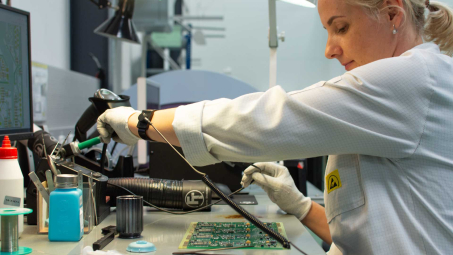
Step Eleven: The PCB Plating Process
Once the PCB has been cleaned after the drilling process, it undergoes chemical treatment. During this process, a very thin layer of copper, just a few microns thick, is applied to cover the uppermost layer of the board and fill the recently drilled holes. Without the plating process, these holes reveal the fibreglass substrate within the panel.
The plating process serves multiple functions. It helps protect the outer layers of the PCB from moisture, contamination, and oxidation. They improve the aesthetics and the soldering of the PCB, as well.
Step Twelve: Outer Layer Imaging and Etching
After imaging the outer layer with photoresist, a protective layer of tin is plated over the copper. The etching procedure eliminates any unwanted copper and residual resistance, leaving just the required copper design.
A protrusion of a few millimetres might cause issues when the device the PCB is intended for is assembled. This is why this step is important to make sure all measurements of the PCB layers and their components adhere to the initial blueprint.
Step Thirteen: PCB Surface Treatment and Finishing
In this step, the PCB undergoes a series of surface treatments. Initially, a solder mask is applied. It is necessary to prevent oxidation and erosion while also preventing conductivity among the solder pads.
Following the application of the solder mask, the PCB is cured at high temperatures in an oven. Next, important information is printed on the board's surface like the board's serial number, origin, etc. After that, a surface finish is applied to prevent oxidation. The specific finish applied to the PCB is determined by design specifications - engineers pick among several options depending on the complexity of the PCB and the environment it is expected to operate in.
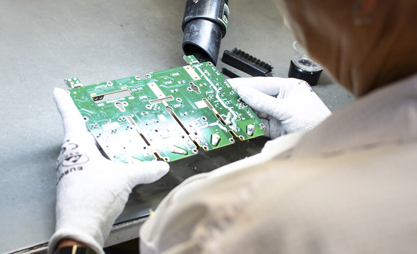
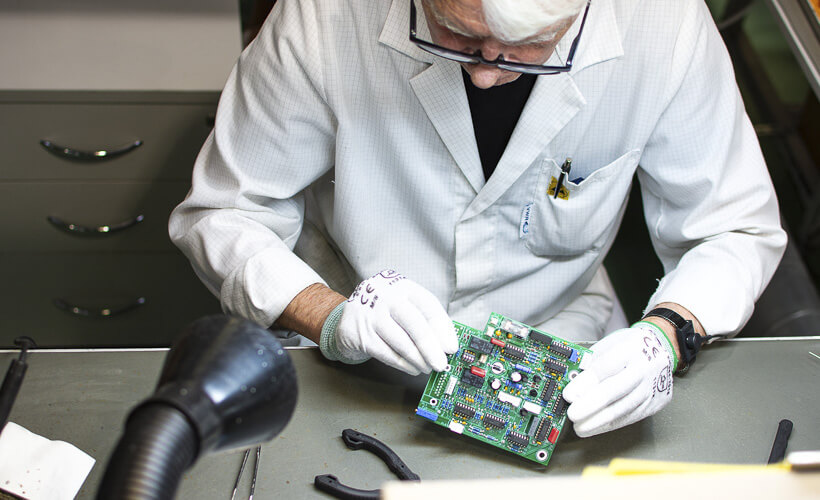
Step Fourteen: Final Quality Assurance and Delivery
We finally arrive at the last stage of the process. Here, the PCB is subjected to a variety of quality tests and inspections to ensure the PCB is ready for operation.
The types and number of tests the PCB is subjected to depend on the type of the PCB. An electrical reliability test, for example, evaluates circuit continuity and isolation to guarantee adequate operation and design conformity.
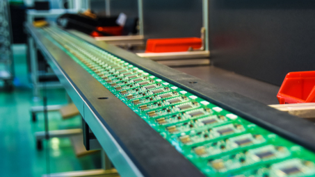
Profiling and routing out methods are used to neatly isolate specific boards. A CNC machine or router is utilized to cut out each board from the panel, shaping and sizing it according to the desired specifications. A thorough final check confirms hole sizes, dimensions, cleanliness, and overall quality.
Finally, before they arrive at their destination to be integrated into electronic devices, the PCBs are rigorously and carefully packed to prevent any damage during storage and transportation. Supply chains are increasingly complex, and the PCB can be shipped across the world before reaching its destination, so the importance of proper packaging can't be overstated.
Contact VECTOR BLUE HUB Today!
VECTOR BLUE HUB is your reliable partner for all of your PCB needs. We specialize in supplying both small and large volumes of high-quality, affordable, and custom PCBs that meet the varied demands of our clients across various industries and sectors. Get in touch now and learn more about our PCB solutions!
Jarosław Krzyżanowski
Jarosław has over fifteen years of experience in electronics manufacturing processes (SMT, THT, AOI, X-RAY, SOLDER WAVE, SELECTIVE, ASSEMBLY). As Process Leader, he ensures an appropriate level of skill in the manufacturing staff, work standards, processes, the appropriate workplace infrastructure, tools and the best use of technological solutions. He gets the most satisfaction out of teamwork. He also likes to look for out-of-the-box innovative solutions our customers require. Music is Jarek’s greatest passion; he also loves family walks and DIY.