


The Multilayer PCB: What it is, how it works, and when you should use it

In the world of electronics, where technological advancements occur rapidly, the multilayer PCB has established its dominance. Over the past few decades, multilayer printed circuit boards have become an indispensable part of modern electronic devices, enabling them to meet the complex needs of today's consumers.
Whether you are a newbie in this business waiting to launch a new product or an experienced electronic company, dive into this article in which we explain the intricicaties of multilayer PCBs.
Table of Contents
- From Single to Double-sided PCB to Multilayer PCB
- What is multilayer PCB?
- Why are multilayer PCBs used?
- Structure and Composition of Multilayer PCBs
- Layers Upon Layers: The Anatomy of a Multilayer PCB
- Manufacturing Multilayer PCBs
- Advantages of Multilayer PCBs
- Multilayer PCB Applications in Modern Technological Domains
- Let's start your journey with the use of multilayer PCBs together!
From Single to Double-sided PCB to Multilayer PCB
Traditionally, printed circuit boards had only a single layer of conductive material. However, a need for double-sided PCBs arose as electronic components grew in number and complexity.
These double-sided boards, with two conductive layers (typically top and bottom layers), provided more space for electrical connections. Soon after, the concept of multilayer PCBs was introduced, revolutionizing the electronics industry.
What is multilayer PCB?
A multilayer PCB, or Printed Circuit Board, is an advanced type of circuitry that facilitates complex electronic functionalities within a compact framework.
Imagine a sandwich, but instead of bread and fillings, you have layers of conductive copper separated by insulating materials. This clever design packs more circuitry into a smaller footprint, making our devices sleeker and more powerful.
This architecture optimizes space and ensures reduced electromagnetic interference, leading to enhanced performance.
Why are multilayer PCBs used?
One of the standout attributes of multilayer PCBs is their enhanced electromagnetic shielding capabilities. These PCBs effectively mitigate electromagnetic interference by integrating internal layers dedicated to ground or power planes, ensuring optimal signal quality.
This meticulous layering also improves signal transmission speeds, reducing cross-talk between tracks and achieving unparalleled design flexibility. Designers can allocate tracks, components, and power planes adeptly, tailoring their designs to diverse electronic requirements.
These PCBs play a pivotal role in noise reduction thanks to their intrinsic design, which fosters noise isolation between the layers. Furthermore, their construction promotes a more streamlined assembly process, effectively diminishing the need for interconnecting harnesses.
All these factors contribute to delivering electronics that are not only compact and lightweight but also reliable, underscoring the pivotal role of multilayer PCBs in the EMS domain.
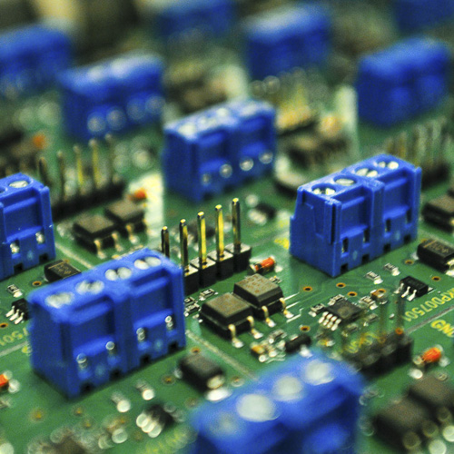
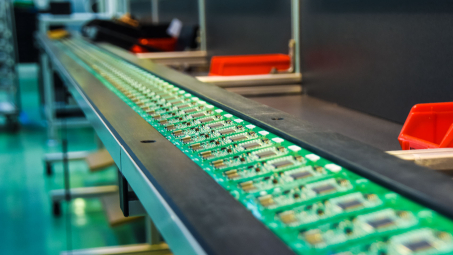
Structure and Composition of Multilayer PCBs
A multilayer PCB board consists of multiple single-layer PCBs stacked upon each other. The foundation of these multilayered PCBs begins with the inner layer core. This core is surrounded by alternating conductive copper layers and insulating material. For electrical connection between these layers, copper-plated holes are utilized.
The outer layers of the board are primarily used for connecting electronic components, while the inner layers handle various functions like signal transmission or power distribution.
Layers Upon Layers: The Anatomy of a Multilayer PCB
The term "multilayer" doesn't simply mean three or four layers. In some advanced applications, there can be four to twelve layers or even up to 37 layers!
The outer layer, often covered in a protective material, provides connection points for electronic components. Inner layers are used for myriad functions, with some acting as ground planes, reducing electronic noise, and others functioning as power planes, distributing power efficiently.
Copper thickness is varied based on the specific requirements of the electronic device in question.
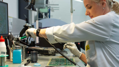
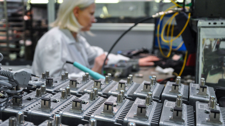
Manufacturing Multilayer PCBs
The complexity of multilayer PCB manufacturing lies in ensuring that each of the multiple layers of conductive material aligns perfectly with one another. This can be achieved through a meticulous lamination process.
The copper foil sheets and insulating layers are stacked together, and a heated hydraulic press applies high temperature and pressure to bond these layers, achieving the desired thickness. Precise drilling processes follow, creating holes for electrical connections between the layers.
Advantages of Multilayer PCBs
Multilayer PCB advantages are manifold. Grasping these benefits can guide informed decision-making in product development, ensuring optimal design choices, cost-effectiveness, and the creation of devices that meet the increasing demands of today's technological landscape.
Advantages:
- High Density: They can accommodate more components and connections in a smaller space.
- Enhanced Signal Integrity: The multiple layers can shield and separate the signals, preventing interference and ensuring optimal signal transmission.
- Flexible Construction Techniques: Multilayer PCBs offer designers a myriad of options in terms of copper thickness, number of layers, and more.
-
Greater Functionality: With the capacity for power planes, ground planes, and multiple signal layers, these boards can meet the intricate needs of advanced electronic devices.
Multilayer PCB Applications in Modern Technological Domains
From smartphones to aerospace technology, multilayer printed circuit boards play a pivotal role. With the world moving towards miniaturized yet robust devices, the demand for multilayer PCBs is growing exponentially.
Their capacity to support multiple connectors and ensure stable electrical connections makes them irreplaceable.
The multilayer PCB applications in several contemporary technological areas are noteworthy:
- Smart Metering: As energy grids become smarter and more interconnected, there is an increasing need for precise data collection and real-time communication. Their compact design aids in integrating multiple functionalities like GSM modules, power measurement circuits, and user interfaces in a single metering device.
- Telecommunications: With the rapid evolution of telecommunications, especially in the era of 5G and beyond, devices require circuitry that can handle high-frequency signals without interference. Multilayer PCBs, with their enhanced electromagnetic shielding capabilities, are vital in devices like base stations, routers, and modems. Their ability to reduce cross-talk and electromagnetic interference ensures reliable and high-speed data transmission.
- Industrial IoT: The IoT revolution hinges on interconnected devices that can process vast amounts of data and make real-time decisions. From sensors in manufacturing plants to automation controllers, multilayer PCBs provide the required computational and communication capabilities in a compact design, enabling the creation of smart factories and enhanced industrial processes.
- Communications Technologies: Beyond traditional telecommunications, the broader domain of communications technologies – encompassing satellite communication, marine communication systems, and more – is witnessing an exponential increase in data flow.
- Computers and Laptops: The motherboards in these devices often use multilayer PCBs to integrate high-speed processors, RAM, and other essential components, ensuring efficient data processing and multitasking capabilities.
- Industrial Controls: Multilayer PCBs are vital in automation equipment, CNC machines, and robotic systems to ensure efficient processing and control.
Summarizing, any advanced electronic device or system seeking to combine intricate circuitry, reliability, and space optimization is likely to leverage the capabilities of multilayer PCBs.
Let's start your journey with the use of multilayer PCBs together!
The multilayer boards represent the pinnacle of printed circuit board evolution. Through the marriage of advanced manufacturing techniques and cutting-edge design principles, these boards meet the exacting demands of today’s electronics, promising a future where possibilities in electronics design are boundless.
VECTOR BLUE HUB rich experience positions us at the forefront of the electronics industry, adeptly navigating the complexities and nuances of multilayer PCB-based device production.
If you're looking to harness the power of multilayer PCBs in your projects, don't hesitate to contact us. Our team is ready to guide and collaborate with you on your next venture.

Jarosław Krzyżanowski
Jarosław has over fifteen years of experience in electronics manufacturing processes (SMT, THT, AOI, X-RAY, SOLDER WAVE, SELECTIVE, ASSEMBLY). As Process Leader, he ensures an appropriate level of skill in the manufacturing staff, work standards, processes, the appropriate workplace infrastructure, tools and the best use of technological solutions. He gets the most satisfaction out of teamwork. He also likes to look for out-of-the-box innovative solutions our customers require. Music is Jarek’s greatest passion; he also loves family walks and DIY.