PCB test: What it is and how it helps identify and solve problems
Which PCB testing method is right for you? Learn about different quality assurance and reliability techniques in this comprehensive guide.
In the fast-paced realm of electronics, the dependability of a product is intricately linked to the quality of its Printed Circuit Boards (PCBs). Ensuring the correct functioning of PCBs goes beyond simply avoiding costly failures and ensuring customer satisfaction; it's about the balancing cutting-edge testing techniques with the practical experiences of engineering. In the general standard of testing, methods such as automated optical inspection (AOI), in-circuit testing (ICT), flying probe testing and X-ray inspection are integrated.
This article delves into how our unique approach to PCB testing – including the hybrid ICT and Functional Circuit Testing (FCT) method – not only meets but exceeds industry standards. The key to superior PCB quality lies not only in the application of these advanced testing methods but also in their strategic integration with real-world engineering insights.
Through this article, we aim to demonstrate how this blend of technology and expertise shapes the future of PCB testing, ensuring unparalleled product reliability and performance.
Essential PCB testing techniques in VECTOR BLUE HUB
Testing of Printed Circuit Boards (PCBs) is an integral aspect of the manufacturing process, crucial for validating the functionality and reliability of circuit boards.
In PCB testing, we distinguish key methods such as:
- Automated Optical Inspection (AOI)
- In-Circuit Testing (ICT)
- Flying Probe Testing (FPT)
These methods are employed to meticulously detect any faults in electronic components, solder joints, and potential circuit irregularities. These techniques are vital in ensuring that the final product aligns with the highest quality standards.
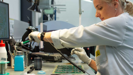
In addition to these, at VECTOR BLUE HUB, we implement a hybrid approach of ICT and Functional Circuit Testing (FCT), a strategy developed from our extensive experience. This hybrid approach not only inspects passive components like resistors, capacitors, and inductors for shorts and opens but also verifies that each component is in accordance with the Bill of Materials (BOM) and functions as intended in the final product. The integration of FCT allows for a comprehensive assessment of every feature and parameter of the PCB, ensuring that each component is correctly mounted and performs its intended function.
Moreover, we emphasize the importance of X-Ray Inspection in the New Product Introduction (NPI) phase, which allows our operators to see beneath integrated circuits, verifying correct cable and connector assembly and identifying potential errors early in the process.
Automated Optical Inspection (AOI)
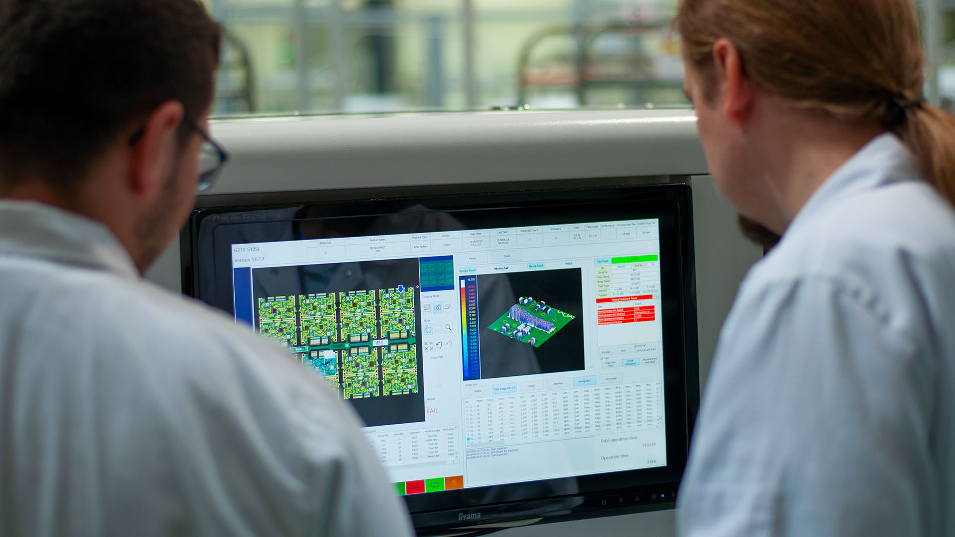
Another key technique in our toolbox is Automated Optical Inspection (AOI). AOI is a non-contact visual inspection method that employs sophisticated single 2D or dual 3D cameras to capture images of the PCB.
These images are then compared against a detailed schematic to detect faults and quality defects. While AOI does not power up the board and may not provide complete coverage for all types of components, its ability to be implemented at any stage of the production process, especially after reflow soldering – where most errors occur – is invaluable. For optimal results, we recommend pairing AOI with other testing methods, such as manual visual inspection, to ensure comprehensive quality control of PCBs.
In-Circuit Testing (ICT)
In-Circuit Testing (ICT) is a robust PCB testing method that utilizes fixed probes to meticulously validate electronic component functionality and solder connections. ICT can be executed using a bed of nails test fixture, but design-for-manufacturing principles are essential to ensure the necessary test point are present. What sets ICT apart is not only its comprehensive fault detection but also its ability to provide precise guidance for addressing any defective PCBs that may come to light during the testing process.
ICT excels at pinpointing a wide range of PCB component faults, including circuit opens, short circuits, and other defects, while also offering clear guidance for handling defective PCBs. This versatile testing approach is instrumental in ensuring the quality and integrity of circuit board assemblies.
Flying Probe Testing (FPT)
Flying Probe Testing (FTP) for PCB testing, a method renowned for its versatility and cost-effectiveness, particularly in low-volume or prototype scenarios. FPT, a fixtureless in-circuit test, utilizes movable probes that navigate across the PCB, testing at various points according to a pre-programmed route.
Importantly, FPT's adaptability allows it to test different boards without the need for specialized fixtures, making it an ideal choice for low-volume production. Although FPT is slower compared to traditional ICT, its flexibility in programming is a significant advantage.
Advanced PCB inspection methods
Diving deeper than standard PCB testing practices, VECTOR BLUE HUB incorporates advanced inspection methods like X-Ray Inspection and Burn-In Testing. These techniques are crucial for uncovering concealed features and potential failure points that basic tests might miss. While these methods are more time-consuming and costly, they provide invaluable insights, ensuring the utmost reliability of PCBs
X-Ray Inspection
At VECTOR BLUE HUB, X-Ray Inspection is an integral part of our New Product Introduction (NPI) process. This technique provides our operators with a revealing glimpse beneath the surface of integrated circuits.
X-Ray Inspection isn’t just about peering into the hidden layers of PCBs; it also plays a critical role in verifying the integrity of cables that are an integral part of certain PCB designs, ensuring they are correctly crimped and positioned within the overall structure. This method is invaluable for implementing corrective actions. By highlighting even the minutest of errors beneath the ICs, we can guide our operators to not only identify these issues but also to learn from them, enhancing their precision in future assemblies.
Moreover, we tailor our approach to meet specific client needs, offering X-Ray Inspection services upon request. This flexibility allows us to cater to unique project requirements, ensuring that each PCB we test meets both our rigorous standards and the specific expectations of our clients. Through this process, we don't just inspect; we improve, turning each X-Ray analysis into an opportunity for refinement and perfection in PCB manufacturing.
Burn-In Testing
At VECTOR BLUE HUB, Burn-In Testing transcends the conventional scope of PCB testing. Here, we apply this rigorous process not just to the circuit boards, but to the finished products in their final form. This approach involves powering up the complete product, sometimes triggering specific functionalities it's designed to perform. The duration of this test can vary – sometimes an hour, other times several hours, or even a full day. Throughout this period, we closely monitor various product parameters.
What sets our Burn-In Testing apart is its focus. Rather than checking every functionality of the product, we concentrate on verifying the integrity of solder joints and ensuring components don't overheat under operational stress. This method is crucial for detecting early-stage characteristics that might lead to failures in the long-term, potentially years into the product's life.
PCB functional testing and qualification
At VECTOR BLUE HUB, ensuring that PCBs not only meet industry standards is at the forefront of our testing process. Our approach integrates functional testing with compliance to quality standards, a key factor in achieving reliability and success in our products. Functional testing is conducted on final products containing PCBs in an environment that closely simulates real-world operating conditions, allowing us to assess how these products will perform under actual usage scenarios.
Our commitment to these rigorous processes and standards means that every PCB we design and produce aligns with the highest quality and performance benchmarks. This is especially critical in industries requiring double verification, like medical, aviation, and transportation, where the reliability of PCBs is paramount.
Functional Testing (FCT)
Our experience has shown that Functional Testing (FCT) is essential, as it not only meets our internal requirements but also aligns with our clients' expectations, going beyond conventional quality control measures. This critical final step involves simulating the actual operating environment of the PCB, ensuring that every component performs as expected in its final application. Our hybrid approach, which combines ICT for verifying passive components like resistors and capacitors, with FCT for testing the overall functionality, allows us to conduct a thorough and accurate assessment of the PCBs.
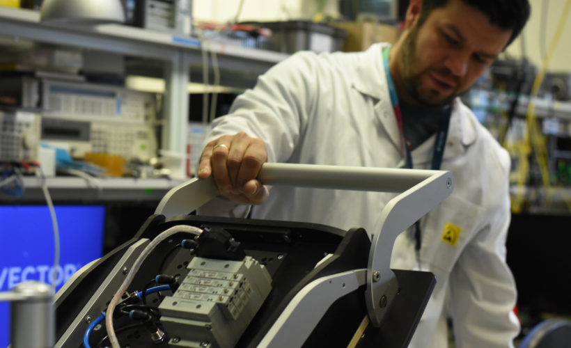
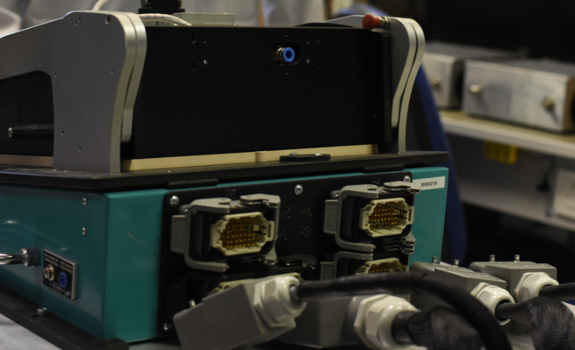
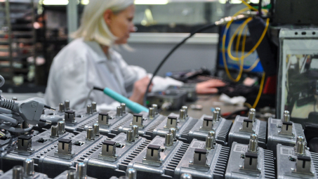
The FCT process at VECTOR BLUE HUB is meticulously designed. We use specialized fixtures and testing software, developed in-house, which allows us to apply various electrical, optical, and RF signals to the PCB through precisely positioned probes and cable bundles. This setup, which can be automated or manually operated based on customer requirements, ensures that every aspect of the PCB is tested under conditions that mirror its intended use.
While FCT can be intricate and time-intensive, it is indispensable for validating the performance of our PCBs in real-world settings. Our commitment to this comprehensive testing ensures the highest level of product dependability for our clients, upholding VECTOR BLUE HUB’s reputation for excellence in PCB manufacturing and testing.
PCB testing best practices at VECTOR BLUE HUB
In the final stage of our manufacturing process at VECTOR BLUE HUB, where prototyping and the New Product Introduction (NPI) phase are completed, we focus on optimizing our PCB testing processes. This optimization is crucial in the mass production phase, ensuring that each product, whether it's an original idea or a redesigned version, undergoes thorough testing.
Test fixture design
Our test fixture design is uniquely tailored to each product's profile, reflecting our extensive product portfolio. These fixtures, semi-passive tools, are crucial for accurately positioning the PCB for testing. Depending on our clients' requirements, these fixtures can be operated manually or automatically, adapting to different product designs and testing needs.
This flexibility in fixture design allows us to ensure precise testing, especially when validating that the PCB aligns with the Bill of Materials (BOM) and is functionally ready for further tests.
Software and automation in testing
At VECTOR BLUE HUB, we employ specialized testing software, designed to cater to the capacity and forecast of our clients. This software, integral to our testing platforms, is crucial in automating the testing process, particularly in our hybrid approach of ICT and FCT. Our testing infrastructure, akin to the 'brain' of the entire system, includes a universal tester with a PC where the testing software is installed. This setup allows us to efficiently load firmware and conduct tests tailored to each PCB.
Functional testing and reporting
We conduct 100% functional testing of devices (DUTs) without sampling, ensuring that every component and feature of the product meets its intended parameters. Post-testing, we provide our clients with detailed test reports. These reports, standard in our practice, have proven invaluable over time, even years after the equipment's usage.
Specialized testing techniques
Our approach includes specialized testing methods like X-Ray Inspection, particularly used in the NPI phase, and Burn-In Testing, applied to finished products. The X-Ray Inspection allows us to see beneath integrated circuits and verify cable crimping, while Burn-In Testing involves powering the product and checking for any overheating or soldering issues, simulating the product's operational mode for extended periods.
Summary
In summary, the meticulous PCB testing at VECTOR BLUE HUB is not just a procedure, but a testament to our dedication to excellence. Our fusion of essential and sophisticated techniques like AOI, ICT, FPT, X-Ray, and Burn-In Testing ensures that each PCB we handle surpasses standard performance metrics.
This innovative approach in test fixture design, strategic test point placement, and cutting-edge software automation elevates the efficiency and precision of our testing processes. In essence, VECTOR BLUE HUB's PCB testing journey - blending advanced techniques with precision engineering - is more than just a process; it's our signature for excellence in electronic manufacturing. Here, each circuit board is not just tested; it's a promise of quality and reliability, setting a new benchmark in the industry.
Frequently Asked Questions
What are the most popular PCB testing methods?
The most popular PCB testing methods are Automated Optical Inspection (AOI), In-Circuit Testing (ICT), and Flying Probe Testing (FPT).
What is the main advantage of Automated Optical Inspection (AOI)?
Automated Optical Inspection is a valuable tool for detecting faults and quality defects in PCBs quickly and cost-effectively, without the need for contact. It can be used as part of a broader testing strategy to improve accuracy.
How does In-Circuit Testing (ICT) work?
In-Circuit Testing utilizes fixed probes to verify electrical components and soldered connections, making it a reliable testing method for printed circuit boards.
Why is Burn-In Testing important?
Burn-In Testing is an important process which helps to detect component failures before they occur, as well as ensuring the reliability of PCBs under various temperature and humidity conditions.
What are some best practices for PCB testing?
Effective test fixtures, optimized test points and probes, and testing software and automation are essential best practices for successful PCB testing.



Mateusz Kowalczys
Mateusz was granted Master of Science at University of Technology of Gdańsk in Electronics and Telecommunication and the ISTQB certificate as a software tester. In VECTOR BLUE HUB, he is the bridge between design and quality, keeping the latter in attention especially during large product volumes. In his over 12 years of experience, he worked on RF and telco projects in the electronic manufacturing services. As a leader, he places honesty and fair cooperation above other things. As a father, he values the time with his daughters. Sometimes he escapes into the mountains, reaching higher and longer trails to finally, one day, get to the Himalayas – that’s his dream.