

X-ray inspection – why it is important?
Compaction of the components constituting electronic devices advances owing to the demand for the comfort of life and work, and also for sparing time. Devices have to be smaller, faster, more accessible and friendlier in terms of user experience. To be sure they will keep working for years we need to look them through – literally. X-ray inspection of the BGA soldering or joints on PCBs finds the smallest defections whose diameter may take no more than one micrometer… The accuracy of its quality control is, thus, spectacular. Is spectacular in this case becoming a standard? And why X-raying electronics saves money?
Let us recall our cellphones ten years ago and compare them to those tiny computers in our pockets, not rarely of greater performance than the big blocks under our desks could ever reach back then. The latter’s components could be seen as they were assembled. In the highly advanced technology, though, where layers of electric connections cram densely on a scanty surface and often overlap themselves, human eye feels lost. X-ray inspection is a safe way to visualise parts that are typically hidden from view.
Moreover, making a tiny mistake in such a tangle can put the whole device on the line. X-ray inspection for PCB Assembly does not leave a choice for producing the cutting-edge electronics as the costs of later servicing might be tremendous, if not overwhelming for the producer. It does save money as this is one of the tools which contribute to the quality control standard of a company. And the optimum quality is everything we want before launching anything on the market.
X-ray inspection irreplaceable in the factory
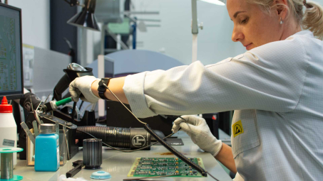
A single electronics component in a high-tech device can be comprised of: flip chips, BGAs, QFNs and other which all land on a printed circuit board (PCB) packed tightly. And only then – in its full functionality and when assembled – it is ready to go under the examination. Micrometre by micrometre an engineer follows each thread of the conductive tracks proving that the electronic device will work errorlessly.
The process does not only assure of the future device’s reliability but also goes into the deepest parts of a component noninvasively. Thus, all kinds of electronic components in their full assemblage are ready for this kind of test right on spot.
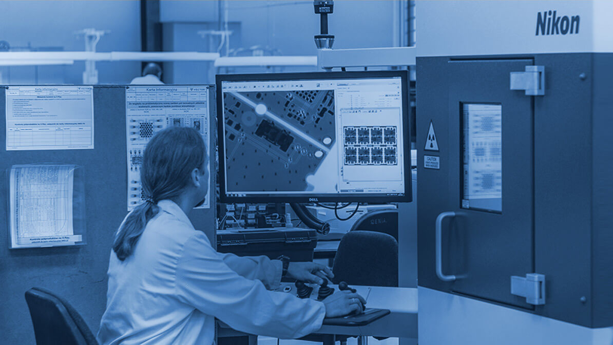
“In other tests, like the electric ones, when an integrated circuit burns or it gets a short, many things come as a potential cause. So you step back in the process, take to searching the damaged part and, at the end, try to mend the flaw in the whole series, which takes a ton of time – especially in complex projects. However, in X-ray imaging, the engineer foresees these situations with the accuracy that allows them to point the problem on the spot because he or she sees it. You take a look inside the device and you see it!” says Jarosław Krzyżanowski, PCB Assembly Process Leader.
The greatest advantage of imaging via X-ray is, in truth, how the machine works. It is analogical to the legacy PCBs with the less condensed structure where an engineer could just see everything. Nowadays, along with condensing electronic installations, the same engineer should still have the same comfort of… seeing. The X-ray inspection makes this comfort possible.

X-ray on the production line or off?
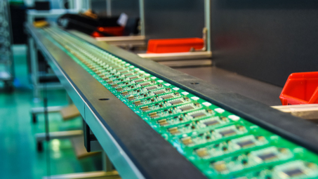
Quick flowing through the whole series of a device and skimming the results of high resolution images make X-ray imaging also accessible. Mass production volumes may get advantage of on-line imaging working on the fly as the production proceeds. That is also the case for PCBs with area array packages, like BGAs, where the number of joints and leads are plenty and their number is multiplied by hundreds. Small and medium volumes trail through the production line with their X-ray pit-stop at the off-line station. An X-ray chamber examines, then, only the chosen samples and allows for the production to keep going smoothly. If a flawed sampled comes under the X-ray tube, the whole series is revised and the testing process starts again with the next new batch and batch sample.
Sometimes, the complexity of a component is so multilayer that only the human-support inspection may be considered. In this case, of leads and solderings which hole up beneath packages or parts of greater atomic density, the X-ray tube finds the rescue in the sample operation platform which can tilt. That allows to get 3D image thanks to which the examining engineer can peep behind the troublesome elements. 3D imaging is generated by a series of 2D takes from the angles around what results in receiving a structured block. Anyone can infer that the production line, if the on-line X-ray solution is used, would have to stop for a couple of minutes, so that is not an economic attitude. Assembling would take forever if all components had to undergo the 3D inspection. Then again, the off-line station is an option. Taking a sample from the batch and repeating the test on the next one is the best way to be assured of the reliability of the devices.
What is the standard?
Nowadays, X-ray imaging might be happening as a standard test. The technology is progressing and the tech-savvy of the designers lays more and more compacted and tinier components on the “green” boards.
“The environment we live in, the technology, our needs – all of that bends what we do here to the standard quality. How to reach the same level without X-ray imaging? It’s hard to say, now. So yes, this kind of test is a standard when the producer wants to set the quality right to what is going on around, to what people search using the electronics,” adds Jarosław.